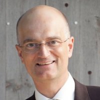
Prof. Dr.-Ing. Peter Wellmann
Prof. Dr.-Ing. Peter Wellmann
Prof. Dr.-Ing. Peter Wellmann
Curriculum Vitae
- 1992: Physics Diploma at the Institute of Technical Physics 1 (University of Erlangen-Nürnberg) working with Prof. Dr. G. Döhler – spektroscopical investigations of InP n-i-p-i doping superlattices.
- 1995: Promotion (Dr.-Ing.) at the Institute for Materials Science 6 – Electronic Materials (University of Erlangen-Nürnberg) working with Prof. Dr. A. Winnacker – rare earth (erbium and ytterbium) doped quaternary InGaAsP semiconductors.
- 1996-1998: PostDoc at the Materials Department (UCSB, University of California in Santa Barbara, USA) working with Prof. Dr. P.M. Petroff – hybride ferromagnet semiconductor systems (synthesis, characterization and device technology) and tuning of self assembled InAs quantum dots.
- 1998-2001: “Habilitation” at the Institute for Materials Science 6 – Electronic Materials (University of Erlangen-Nürnberg) working with Prof. Dr. A. Winnacker – vapor growth and characterization of SiC single crystals.
- 2001: “Privatdozent” (faculty member) at the Institute for Materials Science 6 – Electronic Materials (University of Erlangen-Nürnberg) – vapor growth of wide bandgap semiconductors, semiconductor characterization, spectroscopical investigations of organic semiconductors.
- Jan.-Apr. 2004: Invited Professor at the Institut National Polytechnique de Grenoble (INPG), working with Prof. Dr. Michel Pons – numerical modeling of a modified physical vapor transport reactor for SiC crystal growth and optical characterization.
- Apr. 2006: Invited Professor in the Groupe d’Etude des Semi-Conducteurs (GES) (Université Montpellier 2, France) working with Prof. Dr. Jean Camassel – electrical and optical characterization of SiC.
- 2006: apl. Professor at the Materials Department 6 – Electronic Materials (University of Erlangen-Nürnberg) – – vapor growth of wide bandgap semiconductors (in particular SiC), organic light emitting device (OLED) research, hybrid material composites of inorganic nanoparticles imbedded in organic semiconductors, semiconductor characterization (electrical, optical, structural).
- since 2007: Professor at the Materials Department 6 (i-MEET) – Electronic Materials (University of Erlangen-Nürnberg) – vapor growth of wide bandgap semiconductors (in particular SiC), hight temperature crystallization, thin film solar cell materials (chalcopyrite and kesterite), hybrid material composites of inorganic nanoparticles imbedded in organic semiconductors, semiconductor characterization (electrical, optical, structural), since 2012 treasurer of the German Crystal Growth Association DGKK, since 2012 member of the E-MRS executive committee.

